So to start with a small disclaimer, I have only ever made this one PCB, so I am no expert! Hopefully though this might give people an insight as to how it’s done and maybe encourage others to give it a go.
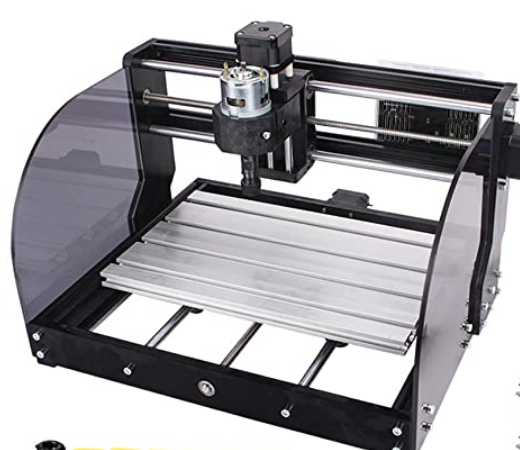
I recently got myself a CNC machine to try this, the 2018 pro with laser attachment:
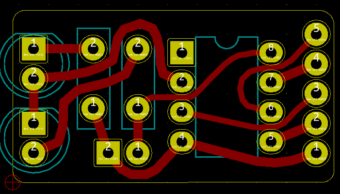
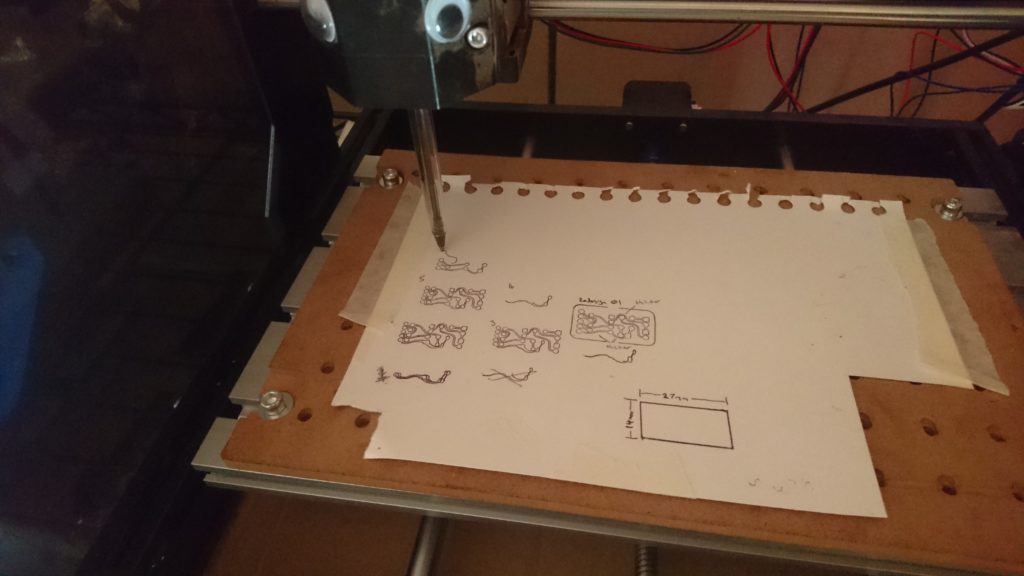
I’m going to presume you’ve already got a design already programmed and working on a breadboard. After that I used KiCad to design the schematic, and from the schematic generated the pcb layout!
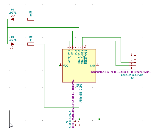
Originally I didn’t widen the traces or make the pads bigger however in retrospect this should have done from the beginning. I ended up using a trace width of 8mm and making the pads 2 mm Thick with a 0.9 mm holes.
From KiCad you will want to export the gerbers for the traces, edge cuts, solder mask and the drill file. These are then imported into Flatcam to generate the gcode files which tell the CNC machine what to do. It is a pain in the arse but hopefully will end up looking something like:
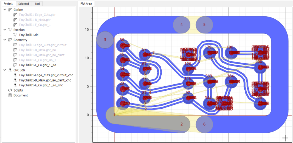
for the “F_CU” and “B_Mask” I ended up telling it I was using a 0.1 V bit with 10° angle. Both the drill holes and the outer edge I ended up using a 0.8 flat bit. When creating the paint area for the B_Mask set the depth to 0.4 as we only want to scrape the very top of the copper to remove the solder mask, instead of going down 0.4 however move the bit up 0.4 and set that position as 0 on the Z axis.
The gerber files generated from flatcam were then sent to “Candle” which controls the CNC machine. Typical me, I figured was all good, set X,Y and Z did a probe and went for it, changing some settings here and there… this is the disaster that I ended up with:
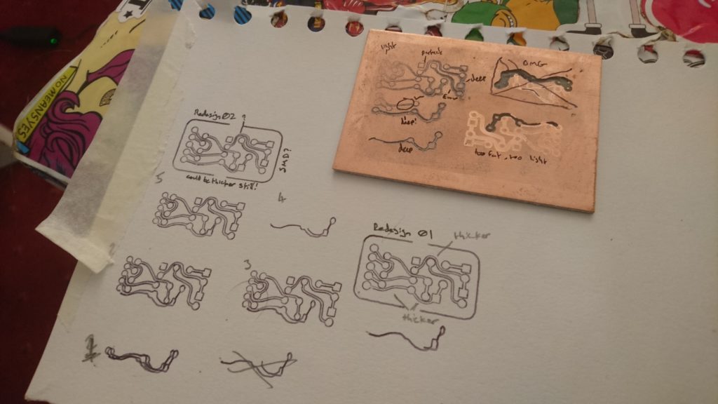
So after drawing it with a pen first I thought it was good enough to carve using the CNC.. I was wrong, the test blank there was me trying to dial in the correct height! eventually I redesigned to use fatter traces and pads and that is “Redesign 02” as drawn above.
Eventually it came out all right.. I ended up setting the bit quite a bit higher than it needed to be and telling the software that that was 0 on the z-axis, and slowly lowering it by 0.01mm at a time until the following was made:
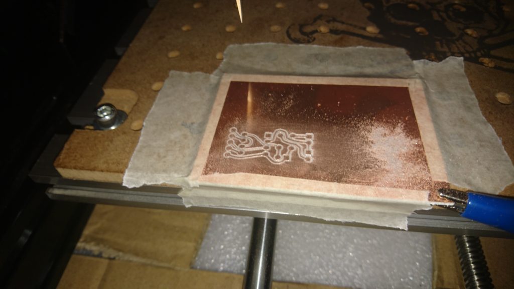
I did create a height map, but recommend not using it for the above v-carve as it seems to cause more issues than it’s worth, however DO make it before and save for later! once I felt the traces were OK I then squirted on what turned out to be too little solder mask:
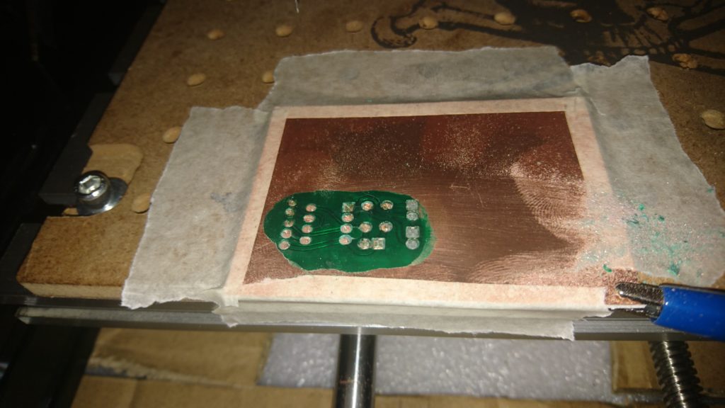
As you can see the pads on the right were carved away! I figured I could bodge this by removing some over a trace and soldering to that instead. This is where you should use the height map to prevent this from happening.
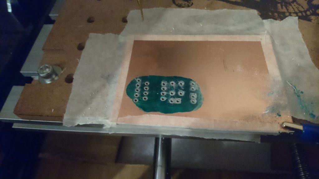
Drill holes were put in the PCB and finally it was cut out from the blank!
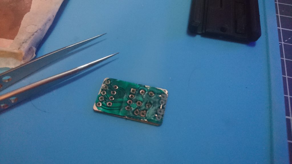
YEY A homemade PCB, granted it’s a bit rough around the edges.. but hopefully this might have helped someone or inspired.
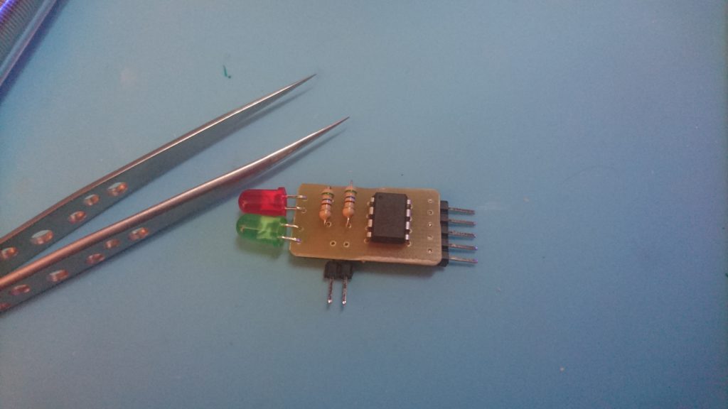
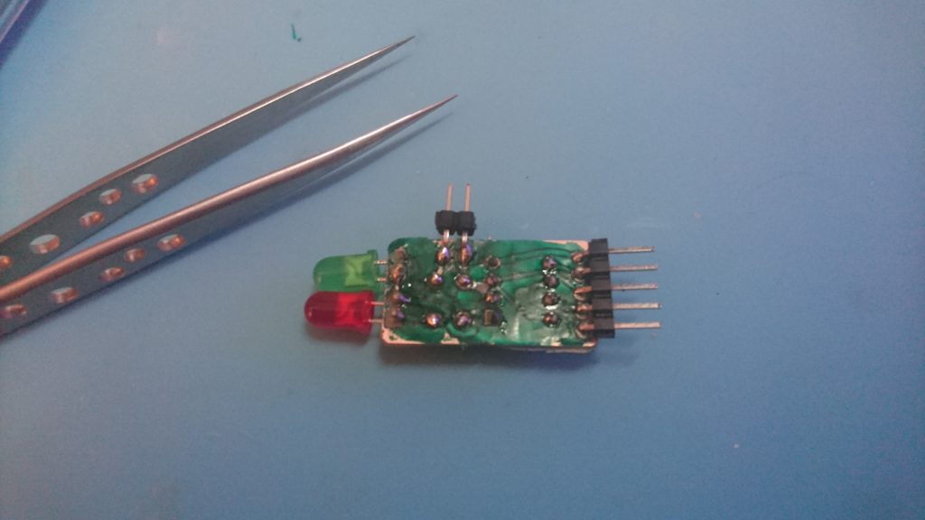
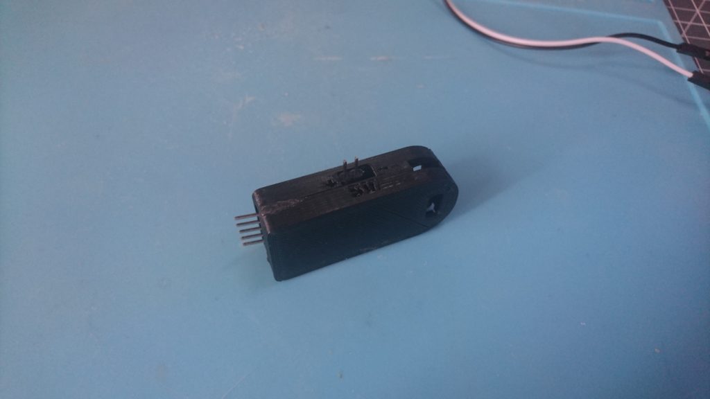
Since we’ve got this far might as well finish it up, lets populate the components.
Lets mock up a case
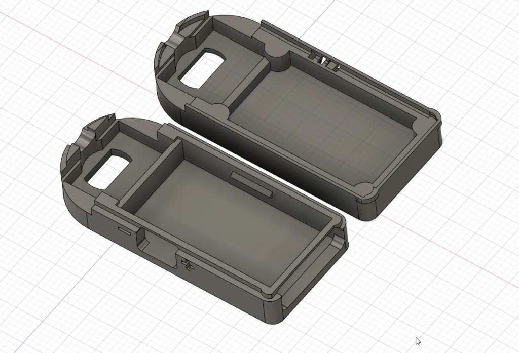
And 3d print it
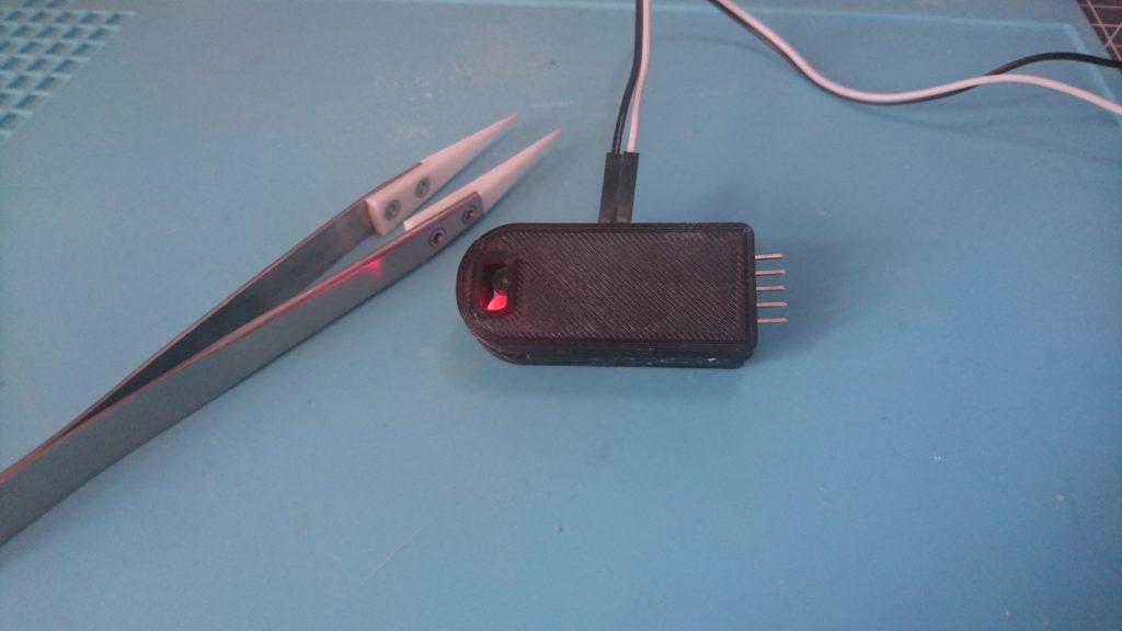
And that’s how you can make a simple prototype in very little time!
